Connect with us

Screen: 6.52 Inch Camera: 13MP RAM: 3/4 GB Battery: 5000mAH Price in Pakistan: Rs.23,999/- Dive into the world of affordable brilliance with the Oppo A16, priced...
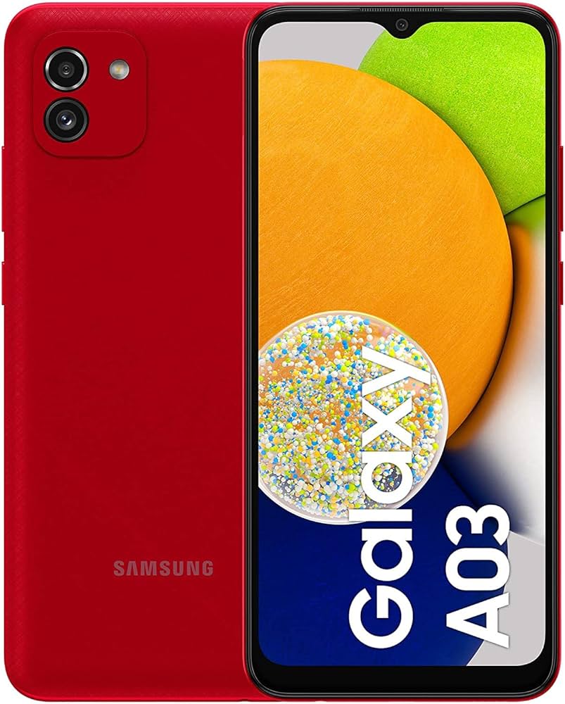
Looking for an affordable yet feature-packed smartphone? The Samsung Galaxy A03 is making waves in Pakistan with its budget-friendly price tag of PKR 27999. Released in...